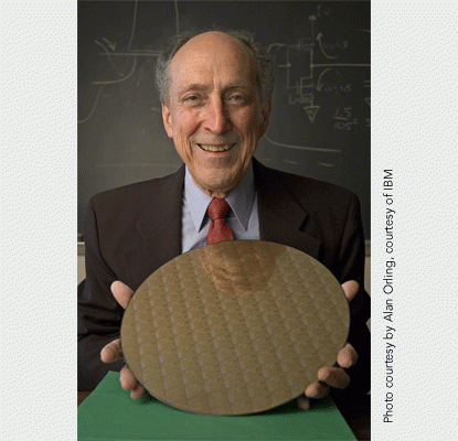
Robert Dennard
Robert Dennard, who grew up in rural Texas and started school in a one-room schoolhouse, says he “had a lot of time to think and read and contemplate.” He recounts that he was always looking for better ways to do things, such as a faster way to chop kindling for the stoves. He later brought this penchant for improvement to IBM, where he developed the one-transistor dynamic random access memory (DRAM)—the paragon for low cost digital memory, ubiquitous in the computer industry today. At IBM, he also developed a significant theory on electronic device scaling, which has been a driving force in microelectronics. For these achievements, Dennard is the 2005 recipient of the $100,000 Lemelson-MIT Lifetime Achievement Award.
In 1966 Dennard was a member of an IBM team doing research on a six-transistor memory cell, and he thought there must be a simpler method to build memory in this technology. His solution evolved as a single field-effect transistor that performed the reading and writing of information stored as an electric charge on a capacitor, now commonly known as a DRAM cell. This technology, patented in 1968, expended less energy and was cheaper than earlier magnetic memory. It was introduced in products on the market in the 1970s and today is the foundation for memory (RAM) in most computer components and systems.
Dennard and his colleagues also conceived the scaling theory, a concept of reducing the dimensions of metal-oxide field effect transistors (MOSFETs) and their interconnecting wires, which led to denser, less expensive and faster integrated circuits, whose properties grew directly proportional to the degree of miniaturization. Dennard published this theory in 1974 in the paper “Design of Ion-Implanted MOSFETs With Very Small Physical Dimensions.” It is now a “Classic Paper” as recognized by the Proceedings of the Institute of Electrical and Electronic Engineers in 1999. The scaling theory, which drives miniaturization in the industry, has enabled computing to be portable, from laptops to cell phones to other technological devices. He has continued to build on the scaling theory over the last 30 years at IBM, where engineers have pushed the edges of the theory’s physical limits.
Dennard received his BS (1954) and MS (1956) in electrical engineering from Southern Methodist University in Dallas, Texas and his PhD (1958) in electrical engineering from Carnegie Institute of Technology in Pittsburgh, Pa., today Carnegie Mellon University. After completing his degrees, Dennard joined IBM , where he continues research today as an IBM Fellow at Yorktown Heights, N.Y. “I wasn’t that involved in really creative things until I came to IBM and they handed me a patent notebook, and they said, ‘put all your ideas in here,’” remarked Dennard. Since 1965, he has been granted 35 U.S. patents in semiconductors and microelectronics.
A member of the National Academy of Engineering and a fellow of the Institute of Electrical and Electronics Engineers (IEEE), Dennard is a recipient of the National Medal of Technology (1988), the Harvey Prize from Technion (Israel, 1990) and the IEEE Edison Medal (2001), among others. He was inducted into the National Inventors Hall of Fame in 1997. According to Dennard, “The most important thing about the inventive process is seeing the problem and asking questions: what if ... we did this, why does this have to be this way ... isn’t there a better way to do it?”